RC Switch by Alan Bond

RC SWITCH
This PICAXE based project was designed for the on/off control of motors (eg bilge bumps, bow thrusters, fire hose pumps etc) or lighting on radio controlled model boats, but will doubtless find application in other radio control projects. The PICAXE chip decodes the receiver signal and at a pre-set pulsewidth switches on a power MOSFET to drive the load. A small amount of hysteresis about the trip-point is included to prevent switch jitter and a user selectable link programs either momentary or latching operation of the switch. The trip point can be set by potentiometer anywhere within the range of the radio control joystick. This allows the unit to be adjusted to operate when some other device controlled by the same receiver channel reaches a certain critical point in its travel.
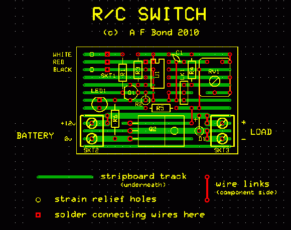
Unlike RC switches utilising relays, the switch "contacts" are not floating to be assigned as you wish - the 'hot side' of the load *must* be wired to the +ve of its power source - and the 'cold' side of the load is switched to 0v by the MOSFET. This is taken care of in the attached layout if up connected as shown. The design is easily adapted to utilise a relay if preferred.
A transistor buffer is used to condition the signal from the receiver. The output voltage swing of some receivers (especially 2.4Ghz types) has been found to be insufficient to trigger the PICAXE 08M (Schmitt Trigger type) input.
An LED is also connected to the gate of the MOSFET to indicate the on/off state of the switch. R4 holds an input port of U1 high unless it is shorted to ground by the jumper link - the state of this port is used to determine whether the switch is to be momentary or latching. R6 serves to reference the source ('earthy' end) of the FET to the PICAXE 0v rail so it may be turned on and off by the chip, but prevents large motor earth return currents flowing in the radio control earth system and forces them to return directly to the battery (via SKT2). D1 protects the MOSFET from high flyback voltage spikes caused by switching inductive loads (like motors).
A *logic-level* N-Channel enhancement power MOSFET must be used if it is to be fully turned on by the 5v swing from the PICAXE chip. No heatsink is shown in the layout and it is instructive for the user to calculate the current capability of the switch. Use the Rds(on) quoted on the spec sheet of the device and calculate i-squared-r watts and look at the device's free-air power dissipation capability at its maximum case temperature. As specified it's quite a few amps! For higher currents a lower Rds(on) device can be used and/or a heatsink employed.
The following guidance is given for those who wish to try developing the PICAXE program for themselves. The values relate to (standard) operation at 4Mhz.
First I sample the potentiometer ('readadc' command) and scale the (0 to 255) result to yield a variable in the range 105 to 195 - this is to set my trip points between 1.05mSec to 1.95mSec. (note: 10uSec pulsewidth reading resolution at 4Mhz). Next I sample the rc signal ('pulsin' command - note the buffer has inverted the input signal so be sure to measure *negative* going pulses) and determine which side of neutral (1.5mSec = 150) it lies. This is because the program logic and hysteresis conditions either side of neutral are different. For ease of understanding I will first describe operation in the 150 to 195 region. Let us assume the trip point is set to 1.7mSec (=170)
For momentary switch operation it is simply a matter of determining if the input signal is greater than 170. If so the output pin driving the FET is set high ('high 0'). On further iterations round the loop, the output pin continues to be set high each time until such time as the input signal is determined to have reduced below 165 (5x10=50uSec of hysteresis) in which case the drive to the FET is now asserted low ('low 0')
Similar logic applies to operation in the 105 to 149 region, except that this time (for e.g. a 1.3mSec trip point) you need to check if the input signal is *less* than 130 to switch on the FET and *greater* than 135 to switch it off again.
For latching operation (as determined by the state of the link) you will need to set a 'flag' to remember which state the switch is in and toggle it accordingly.

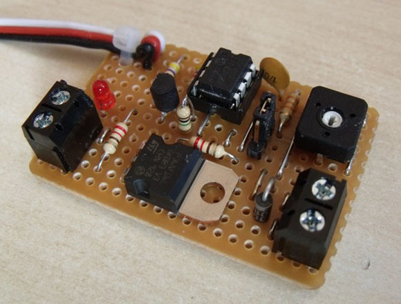
As can be seen from the pictures, the unit is easily constructed on stripboard and a 200mm servo lead is soldered in and strain-relieved with a tie-wrap to provide the input interface. No provision has been made for programming the PICAXE chip in situ, so this must be done elsewhere in a slave rig.
The layout diagram shows the (potentially) heavy current carrying parts of the stripboard track that would benefit from thickening up by running a bead of solder along them
All the parts are available from Technobots of course!
PARTS
R1 - resistor 47k #2008-047
R2 - resistor 1M #2009-010
R3 - resistor 4k7 #2007-407
R4 - resistor 47k #2008-047
R5 - resistor 220R #2006-220
R6 - resistor 220R #2006-220
C1 - capacitor 100nF disc ceramic #2013-100
Q1 - transistor BC337-16 #2300-412
Q2 - power MOSFET STP36NF06L #2300-850 or better
U1 - integrated circuit PICAXE08M #3803-111 pre-programmed chip
IC Socket for U1 #2700-008
D1 - diode 1N4001 #2100-001
LED1 - 3mm light emitting diode, red - #2110-300
RV1 - preset potentiometer 4K7 #2000-405
LK1 - PCB Header 3 way #2700-081
LK1 - PCB Jumper Link #2700-070
SKT1 - 200mm servo lead #3601-008
SKT2 - 16A 2 way terminal block #1208-002
SKT3 - 16A 2 way terminal block #1208-002
stripboard 95x64 #2700-110
